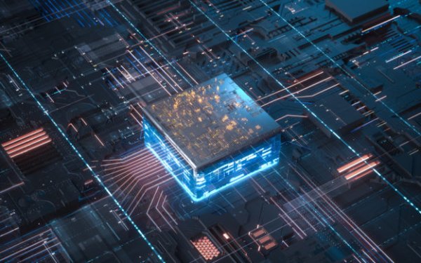
Today, when artificial intelligence (AI) reshapes global technology versions at an unprecedented speed, the combination of high-performance computing (HPC) and AI has become the hottest focus in the market. In this regard, Zhang Yulin, vice presiden...
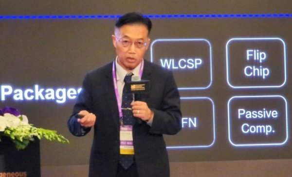
Today, when artificial intelligence (AI) reshapes global technology versions at an unprecedented speed, the combination of high-performance computing (HPC) and AI has become the hottest focus in the market. In this regard, Zhang Yulin, vice president of Micron Advanced Packaging and Testing Operations at Taiwan, said that high-frequency wide memory (HBM) plays a key role in the AI era, and its backdrop comes from extremely challenging advanced packaging technology, especially the unique and future potential of Micron's TCB-NCF (heat pressure combined non-conductive membrane) process.
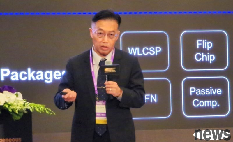
Zhang Yulin said in Semicon Taiwan's theme speech on "HBM and Advanced Packaging in the AI Age" that with the evolution of AI models from GPT-1 to GPT-5, the amount of tokens required for training has shown nearly one million times the amazing growth, and the model parameters have also reached a scale of tens of thousands. This creates an unprecedented desire for the memory. One HBM will consume three DRAM production capacity, which makes the global DRAM supply challenge extremely severe.
In the past, GPUs were connected to GDDR6 memory through PCB board. Today, in order to pursue extreme performance, GPU and HBM memory are placed together on advanced 2.5D/3D stacking platforms such as CoWoS or EMIB. This architecture ensures the shortest circuit and parallel computing capabilities of data transmission, and has achieved a huge improvement in heat dissipation and stability. From the early 4-layer stacking HMC to the 8-layer, 12-layer or even 16-layer stacking HBM3, which is now popular in the industry, shows the market demand for memory capacity, prompting manufacturers to constantly challenge the limits of stacking technology.
Zhang Yulin pointed out that HBM is the shortest distance and most efficient solution to connect memory to processors. He explained that even if the basic unit of the memory uses advanced high-K dielectric materials, it still requires physical space, whether horizontally expanding or vertically stacking. Integrating it into logical chips that use advanced processes such as extreme ultraviolet light (EUV) is not only cost-effective, but also causes leakage problems due to high temperatures, affecting performance. This is exactly why memory, radio frequency (RF) and high-power components need to be integrated through advanced packaging technology rather than simply following Moer's law for slight compression.
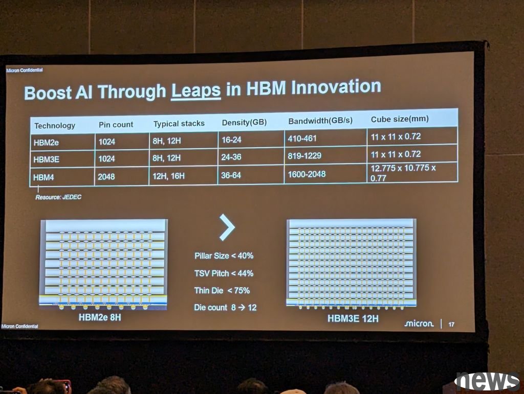
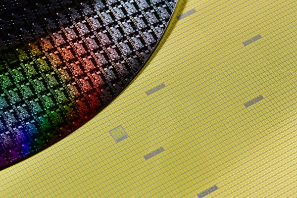
In fact, a 12-inch wafer thickness is about 775 microns, while the thickness of the HBM3 or HBM4 single-layer wafer is less than one percent. Therefore, according to the laws of physics, the stress will increase by eight times when the thickness is reduced by half. If the thickness is reduced to one-twentieth of the original, the stress will be generated 8,000 times that of the amazing one. Therefore, handling such extremely thin, extremely fragile wafers is like carrying out precision construction projects on paper, but it also brings huge technological innovation opportunities to the industry. From HBM2E to HBM3, the pitch is reduced by more than half, while the number of TSVs (silicon perforation) is increased by four times. Behind these data is the fundamental reason for the rapid development of AI performance, and it also brings packaging engineers an extremely "dirty job".
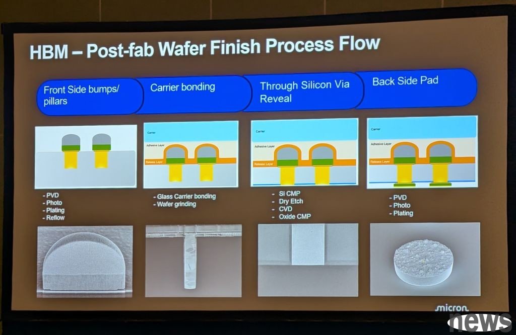
Among the many packaging technology routes, Micron is a few companies that insist on using TCB and NCF processes. Although this route has high requirements for process control, it also brings unique advantages. In particular, compared with the mainstream underfill coating process, pre-filled NCFs can easily control the flow of the glue and the generation of bubbles during the pressure bonding process. If the bottom fill is only based on the hairy bottom, the bubbles are easily trapped inside the wafer; with NCF, we can better discharge the bubbles outward. Once bubbles are generated, it may lead to bridge connection problems that are more minor than the contact itself, leading to short circuits and failures.
Zhang Yulin emphasized that HBM's manufacturing process is a manifestation of Fail Philosophy. From thinning, cutting, stacking to final molding, the entire process involves hundreds of steps. Any minor error in the ring, such as wafer ripping, cracking, or particle contamination, will be amplified during the subsequent stacking process and will lead to the ultimate failure. Therefore, the yield control of the entire process is as difficult as a wire rope.
With its past research and development experience in electronic materials and semiconductor fields for more than ten years, Micron successfully led a team to overcome the challenges of TCB-NCF process, making it successful in the market, and also established a unique technical wall-to-wall for Micron in the HBM field. Therefore, semiconductor industry is at a turnaround point. In the past, the minusculation of Morrow's law was the main force in promoting industry development; today, the investment scale of advanced packaging technology has been comparable to the front-end process, and has become the key to sustained efficiency growth.
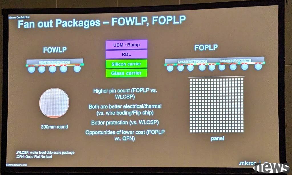
Zhang Yulin finally pointed out that in order to achieve higher speeds, greater frequency widths and lower costs, the industry is developing towards fan-out packaging, more refined RDL (re-line layer), and hybrid bonding. However, these new technologies have also brought new problems, such as reliability challenges such as syrup and electric discharge (ESD). While pursuing a 30% reduction in power consumption or a 30% speed increase, engineers must also face more severe heat dissipation and stress management problems. In the future, new materials, new architecture designs and advanced packaging solutions will be jointly driven. From HBM memory to DRAM, SSD NAND flash memory, and then to low-power DRAM modules, Micron is committed to providing a comprehensive range of memory solutions to meet the massive demands of AI training and recommendations, and plays an indispensable key role in this memory revolution initiated by AI.